
A modern CPU can execute billions of instructions per second, but it cannot perform useful work without access to data and instructions.
Much of this information is stored in system memory, commonly called RAM.
However, a CPU does not simply connect directly to memory chips and read data whenever it wants.
Communication with RAM requires precise timing, address translation, electrical signaling, and coordination.
The hardware responsible for managing much of this communication is called the memory controller.
Understanding how a memory controller works helps explain how processors access RAM, why memory speed matters, and how CPU caches, memory channels, and DDR technology affect computer performance.
What Is a Memory Controller?
A memory controller is a hardware component that manages communication between a processor or another computing device and system memory.
Its primary responsibility is to translate memory access requests into the commands and signaling operations required by RAM.
For example, when a CPU needs data that is not available in its caches, a request may eventually reach the memory controller.
The controller determines how to access the appropriate memory location and coordinates the transfer.
The memory controller performs several important tasks, including issuing memory commands, scheduling requests, managing DRAM timing requirements, and coordinating data transfers.
Modern memory controllers also support features such as multiple memory channels, memory refresh coordination, and error detection or correction where supported by the memory system.
The memory controller is therefore an essential connection between the CPU’s internal memory system and physical RAM.
Where Is the Memory Controller Located?
In older personal computers, the memory controller was often located in a chipset component called the Northbridge.
The CPU communicated with the Northbridge through a system bus, and the Northbridge managed access to RAM.
This arrangement introduced additional communication overhead because memory requests had to travel through an external chipset.
Modern desktop, laptop, and server processors generally use an Integrated Memory Controller (IMC).
An integrated memory controller is built into the processor chip or processor package, depending on the architecture.
This allows the CPU to communicate with memory more directly and can reduce latency while improving bandwidth and power efficiency.
Both AMD and Intel have used integrated memory controllers in their mainstream processor families for many years.
Modern systems-on-chip, including many ARM-based processors, also integrate memory controllers alongside CPU cores and other components.
How Does a CPU Access RAM?
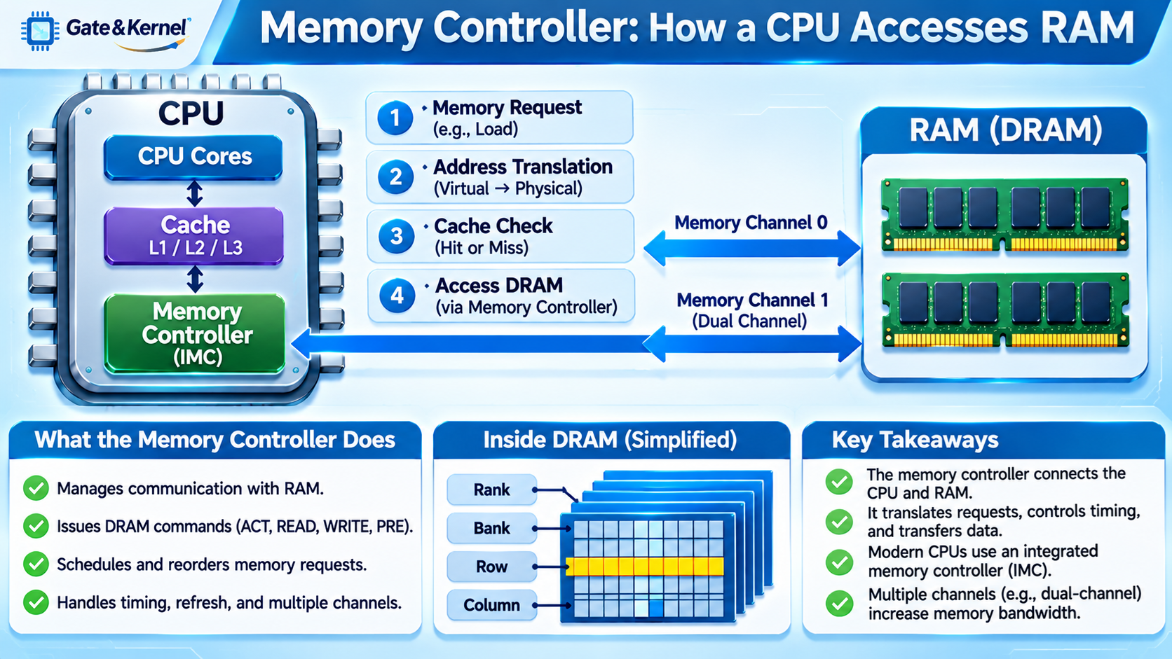
When a program needs information stored in RAM, the CPU follows a series of operations involving registers, caches, address translation, and the memory controller.
A simplified memory read works as follows.
Step 1: The CPU Generates a Memory Request
A running instruction requests data from a particular memory address. For example, a load instruction may request a value from an array stored in memory.
Step 2: The CPU Translates the Address
Most modern operating systems use virtual memory. The CPU’s memory management hardware translates the virtual address into a physical address, often using cached translations in a Translation Lookaside Buffer (TLB).
Step 3: The CPU Checks Its Cache Hierarchy
The processor checks the relevant cache levels, typically including L1, L2, and L3 caches where present.
If the requested data is already available, the CPU can obtain it without accessing system RAM.
Step 4: A Memory Request Reaches the Memory Controller
If the requested data is not available in the cache hierarchy, the processor’s memory subsystem sends a request toward the memory controller.
Step 5: The Controller Accesses DRAM
The memory controller determines the appropriate memory channel, rank, bank, row, and column, then issues the required DRAM commands.
Step 6: Data Returns to the CPU
The requested data is transferred from RAM through the memory interface. It may be placed into the CPU cache hierarchy before the processor uses it.
Actual processors can have many memory operations in progress simultaneously, so the process is more complex than this simplified sequence.
How Is Data Organized Inside DRAM?
Modern system RAM commonly uses Dynamic Random Access Memory (DRAM).
DRAM stores information in memory cells that use tiny capacitors to represent binary values.
These capacitors gradually lose their electrical charge, which is why DRAM requires periodic refresh operations.
DRAM is organized into structures such as channels, ranks, banks, rows, and columns.
A memory controller must understand this organization to access data efficiently.
For example, when the controller needs information from a particular row, it may issue an ACTIVATE command to open that row within a memory bank.
After the row is activated, the controller can issue a READ command to retrieve data from the appropriate column.
The controller may later issue a PRECHARGE command to close the active row before accessing a different row in the same bank.
These commands must follow specific timing rules defined by the memory technology.
The memory controller manages these operations so that data can be transferred reliably.
Why Does RAM Have Latency?
RAM is much slower than the CPU’s internal registers and caches.
Even when a processor operates at several gigahertz, accessing DRAM may require dozens or hundreds of CPU clock cycles, depending on the system and workload.
Memory latency comes from several sources, including request handling, interconnect delays, DRAM command scheduling, row activation, and data transfer.
DDR memory specifications include timing parameters such as:
CAS Latency (CL): The delay, measured in memory clock cycles, between a READ command and the beginning of the corresponding data output under the specified conditions.
tRCD: The minimum delay between activating a row and issuing an appropriate read or write command.
tRP: The minimum time required for precharging a bank before another row can be activated.
tRAS: The minimum time a row must remain active before it can be precharged.
These timing parameters help determine how quickly DRAM can respond to memory requests.
A memory controller must respect them to ensure reliable operation.
What Are Memory Channels?
A memory channel is an independent communication interface between a memory controller and RAM.
Many desktop processors support two independent memory channels, commonly called dual-channel memory.
Using multiple channels can increase total memory bandwidth because the controller can transfer data over separate interfaces.
For example, a single conventional 64-bit-wide DDR4-3200 memory channel provides a theoretical peak data bandwidth of:
3,200 million transfers per second × 8 bytes = 25.6 GB/s.
Two such channels can theoretically provide 51.2 GB/s of combined bandwidth.
Actual performance depends on memory access patterns, controller efficiency, and other system limitations.
DDR5 introduces a different organization. A typical DDR5 DIMM divides its data interface into two independent 32-bit subchannels, excluding additional ECC bits where applicable.
This improves command and access granularity, but it does not mean one DDR5 DIMM automatically provides twice the aggregate data width of a conventional 64-bit DDR4 DIMM.
Server processors may support four, eight, twelve, or more memory channels, depending on their design.
What Is the Difference Between Memory Bandwidth and Latency?
Memory bandwidth and latency describe different aspects of RAM performance.
Memory bandwidth measures how much data can be transferred per second.
Memory latency measures how long it takes for a requested memory operation to produce the required data.
Higher memory bandwidth is particularly useful when applications need to process large amounts of information continuously.
Examples include scientific computing, video processing, integrated graphics, and large-scale data analysis.
Lower memory latency is important for workloads involving frequent dependent memory accesses.
For example, an application that repeatedly follows pointers through complex data structures may be sensitive to memory latency.
A faster memory transfer rate can increase bandwidth, but it does not necessarily reduce every component of memory latency.
Both characteristics matter when evaluating memory performance.
How Does the Memory Controller Improve Performance?
Modern memory controllers do more than simply forward requests to RAM.
They can reorder pending memory operations to improve efficiency while preserving the architectural memory-ordering rules required by the system.
For example, if several requests target an already open DRAM row, the controller may schedule them together to reduce unnecessary row activation and precharge operations.
The controller also coordinates requests across memory banks and channels, allowing multiple operations to overlap when supported.
Other responsibilities may include managing read and write queues, balancing bandwidth usage, coordinating refresh operations, and controlling power-saving memory states.
These techniques help reduce wasted memory cycles and improve effective memory throughput.
However, aggressive scheduling must still respect DRAM timing requirements, data dependencies, and system correctness.
What Is the Relationship Between CPU Cache and the Memory Controller?
CPU caches and memory controllers work together, but they serve different purposes.
CPU caches store copies of recently used or likely-to-be-needed data close to processor execution units.
The memory controller manages communication with the physical RAM system.
When an instruction requests data that is already in L1 cache, the CPU can usually obtain it without involving the memory controller.
If the data is absent from the entire relevant cache hierarchy, a request may eventually reach the memory controller.
The controller retrieves the required information from RAM, allowing the cache system to supply the processor.
This cooperation reduces the number of slow DRAM accesses and improves overall system performance.
It also explains why larger or more efficient caches can sometimes improve performance without changing the RAM’s speed.
Can a CPU Support Any Type of RAM?
No. A processor’s memory controller supports specific memory technologies and configurations.
For example, a processor designed for DDR4 memory cannot automatically use DDR5 memory.
DDR4 and DDR5 differ in electrical signaling, operating requirements, command protocols, and other architectural details.
Even when memory modules appear similar, they may not be electrically or mechanically compatible.
The CPU, motherboard, BIOS or UEFI firmware, and memory modules must all support the intended configuration.
The memory controller also determines supported features such as memory channels, operating speeds, memory capacities, and certain error-correction capabilities.
Some processors support multiple memory technologies, but the surrounding platform must be designed for the selected type.
Before upgrading RAM, it is important to check both processor and motherboard specifications.
What Is Memory Training?
When a computer starts, the memory controller and system firmware must configure the RAM interface.
This process may include memory training, which adjusts signaling and timing parameters to establish reliable communication.
Modern DDR interfaces operate at very high transfer rates, where small timing differences can affect data integrity.
Memory training may calibrate parameters related to signal timing, delays, and electrical characteristics.
This is one reason some computers take longer to start after installing new memory or changing RAM settings.
If training fails, the system may restart, reduce the memory speed, or fail to boot.
Memory stability depends on the processor’s memory controller, motherboard design, RAM modules, and selected operating parameters.
Why Is the Memory Controller Important?
The memory controller plays a critical role in overall computer performance because the CPU frequently depends on information stored outside its internal caches.
A powerful processor can be limited by insufficient memory bandwidth, high memory latency, or inefficient access patterns.
Applications such as databases, scientific simulations, virtual machines, and memory-intensive workloads can place heavy demands on the memory subsystem.
Memory controllers are also important in embedded systems and system-on-chip designs.
For example, an FPGA-based system may use a dedicated DDR memory controller to communicate with external DRAM.
The FPGA logic supplies memory requests through an internal interface, while the controller manages the complicated DDR signaling and timing requirements.
This separation allows digital designers to work with memory without manually implementing every low-level DRAM command.
Conclusion
A memory controller is the hardware responsible for coordinating communication between a processor and system RAM.
It receives memory requests, manages DRAM commands, follows strict timing requirements, and controls data transfers over one or more memory channels.
Modern processors generally integrate the memory controller to provide efficient access to RAM.
CPU caches reduce the number of memory requests, while the memory controller handles the requests that must reach physical DRAM.
Memory bandwidth, latency, channel organization, and DRAM timing all influence how effectively a processor can access data.
Understanding the memory controller reveals an important principle of computer architecture: CPU performance depends not only on how quickly a processor executes instructions, but also on how efficiently its memory system supplies the information those instructions need.