
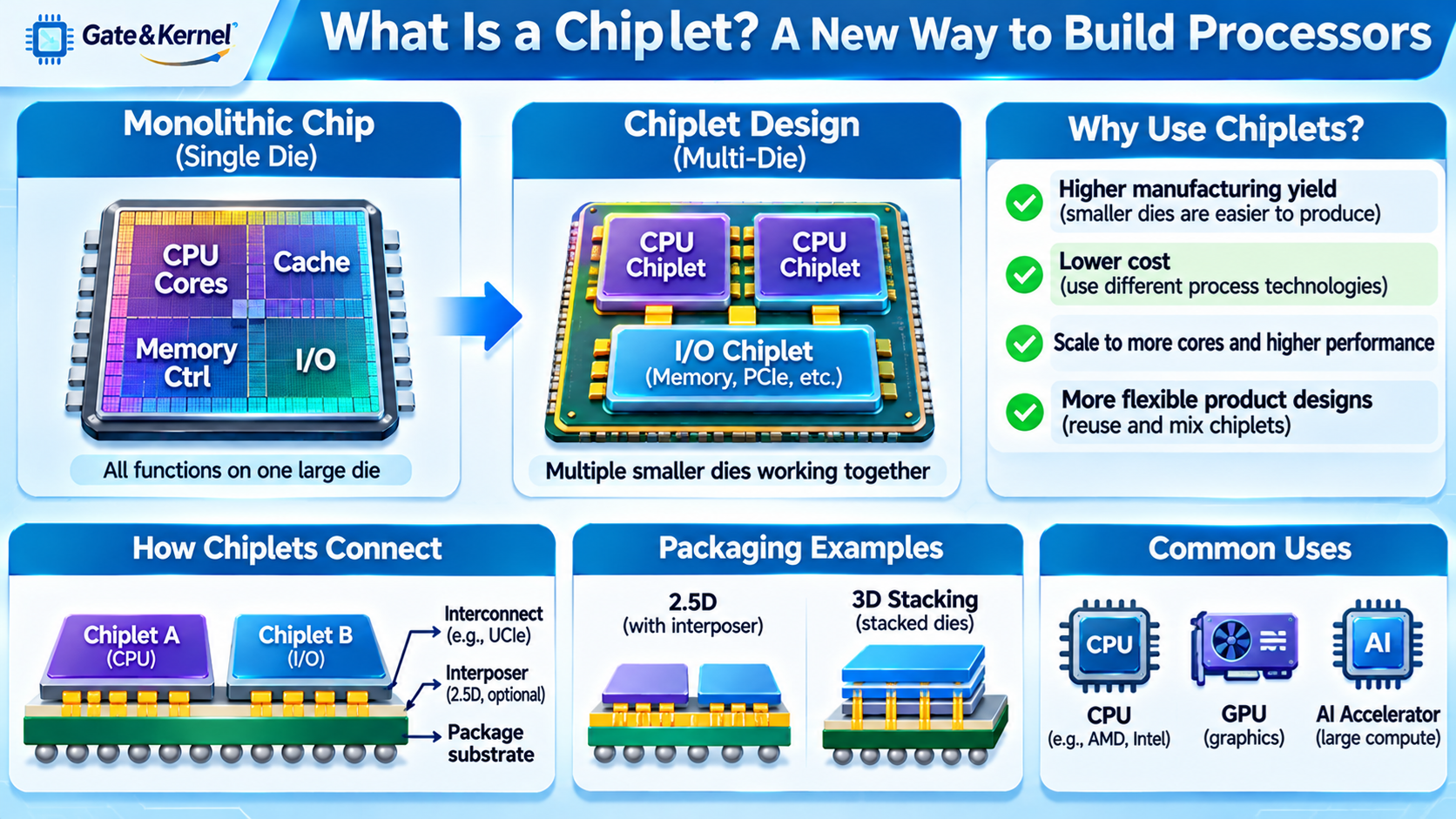
For decades, computer processors were commonly designed as single silicon chips containing CPU cores, caches, memory controllers, and other circuits.
As processors became more powerful, manufacturers continued adding transistors and functionality to increasingly complex chips.
However, manufacturing very large chips presents serious challenges.
Larger silicon dies are more expensive to produce, more difficult to manufacture without defects, and harder to scale efficiently.
One solution is a technology called the chiplet.
Instead of building an entire processor on one large silicon die, engineers can divide the design into several smaller dies and connect them inside a single package.
This approach is changing how modern CPUs, GPUs, and AI accelerators are designed and manufactured.
What Is a Chiplet?
A chiplet is a relatively small silicon die designed to perform a particular function or group of functions within a larger semiconductor system.
Multiple chiplets can be combined inside one package to create a complete processor or system.
For example, a processor might contain separate chiplets for CPU cores, memory controllers, and input/output interfaces.
These chiplets communicate through high-speed connections inside the package.
From the software’s perspective, the complete package may still behave like a single processor.
The main idea is simple: instead of manufacturing one large chip containing everything, build smaller functional pieces and connect them together.
This approach is often called a chiplet-based architecture or disaggregated chip design.
Monolithic Chip vs. Chiplet Design
A traditional monolithic processor integrates most of its major functions onto one silicon die.
For example, CPU cores, caches, memory controllers, and interconnect logic may all be manufactured together.
A chiplet-based processor divides some of these functions across multiple silicon dies.
Consider a processor with 16 CPU cores.
In a monolithic design, all 16 cores could be manufactured on one large die.
In a chiplet design, engineers might use two eight-core compute chiplets connected to a separate input/output die.
Both approaches can provide a 16-core processor, but their manufacturing and engineering characteristics are different.
Monolithic designs can offer short internal communication paths and avoid some die-to-die connection overhead.
Chiplet designs provide greater flexibility in manufacturing, scaling, and combining different technologies.
Neither approach is automatically better for every application.
Why Are Modern Processors Using Chiplets?
One of the biggest reasons for adopting chiplets is the increasing difficulty and cost of manufacturing advanced semiconductor devices.
Modern processors contain billions or even tens of billions of transistors.
As chip designs become larger, several problems become more difficult to manage.
These include manufacturing yield, production cost, chip size limitations, power delivery, and design complexity.
Chiplets offer potential solutions to several of these challenges.
1. Improving Manufacturing Yield
Semiconductor manufacturing is not perfect. Defects can occur during the fabrication process.
A larger silicon die generally has a greater chance of containing a manufacturing defect than a smaller die produced using the same technology.
If a large monolithic processor contains a defect in a critical area, the entire die may become unusable or may need to be sold as a lower-specification product.
Smaller chiplets can be manufactured and tested separately.
Manufacturers can select working chiplets and combine them into a final package.
This can improve usable manufacturing yield and reduce waste.
However, the benefit depends on factors such as chiplet size, defect density, packaging yield, testing cost, and the number of chiplets required.
2. Reducing Manufacturing Costs
Advanced semiconductor manufacturing processes are extremely expensive.
The latest process nodes require sophisticated equipment, complex design tools, and costly manufacturing steps.
Not every part of a processor benefits equally from the most advanced manufacturing technology.
For example, CPU execution cores may benefit significantly from smaller transistors, while certain input/output and analog circuits may not need the same process node.
A chiplet design allows manufacturers to build different components using different manufacturing technologies.
Compute chiplets might use a leading-edge process, while an I/O chiplet uses a more mature and less expensive process.
This approach is called heterogeneous process integration.
It can reduce manufacturing costs compared with producing every component on the most advanced process node.
However, chiplets also introduce additional packaging, testing, and communication costs, so total cost savings are not guaranteed.
3. Building Larger and More Powerful Processors
A silicon die cannot grow indefinitely.
Semiconductor manufacturing equipment uses photolithography to transfer circuit patterns onto silicon wafers.
The maximum area that can be patterned in a single exposure is constrained by the lithography system’s reticle limits.
For many advanced manufacturing processes, a conventional single die is limited to an area of roughly 800–850 square millimeters, depending on the technology and design rules.
Chiplet technology allows engineers to build systems containing multiple dies whose combined silicon area can exceed the size of one conventional monolithic die.
For example, a server processor may combine several compute chiplets to provide dozens or even hundreds of CPU cores.
This modular approach is particularly useful for high-performance computing and data center processors.
4. Creating Different Processor Models
Chiplets can make processor product development more flexible.
A manufacturer may design one compute chiplet and reuse it across several processor models.
For example, a product family could use:
- One compute chiplet for a lower-core-count processor.
- Two compute chiplets for a higher-core-count processor.
- Multiple compute chiplets for a server processor.
The exact configuration depends on the processor architecture and packaging system.
Reusing chiplet designs can reduce engineering effort and simplify the creation of product families.
Manufacturers can also combine chiplets with different capabilities, such as CPU cores, graphics processing, or specialized acceleration hardware.
This modularity is one of the most important advantages of chiplet-based design.
How Do Chiplets Communicate?
Chiplets must exchange data quickly to function as one computing system.
Unlike circuits located on a single silicon die, chiplets communicate through electrical connections that cross die boundaries.
These connections are implemented using advanced semiconductor packaging technologies.
Depending on the design, the chiplets may be mounted on an organic package substrate, connected through a silicon interposer, or integrated using more advanced bridge and stacking technologies.
High-density connections allow chiplets to communicate with substantial bandwidth.
However, die-to-die communication introduces design challenges involving latency, power consumption, signal integrity, and thermal management.
The interconnect must provide enough bandwidth without consuming excessive power or introducing unacceptable delays.
Modern chiplet systems therefore require both sophisticated packaging and carefully designed communication protocols.
What Is 2.5D and 3D Packaging?
Chiplet technology is closely associated with advanced semiconductor packaging.
2.5D Packaging: Multiple silicon dies are placed side by side and connected through a high-density interposer or similar interconnect structure.
The interposer provides fine electrical connections between the dies.
This approach is commonly used in high-performance processors and AI accelerators, especially when a large compute die must communicate with high-bandwidth memory.
3D Packaging: Silicon dies are stacked vertically and connected through short, high-density vertical interconnections.
Stacking can reduce the physical distance between components and improve communication density.
For example, additional cache memory can be stacked above a processor die.
However, 3D integration also creates challenges involving heat dissipation, manufacturing complexity, and testing.
Not every chiplet-based processor uses 2.5D or 3D packaging. Some use conventional package substrates with several dies mounted side by side.
What Is UCIe?
As chiplet technology becomes more common, the industry needs standardized ways for chiplets to communicate.
One important initiative is Universal Chiplet Interconnect Express (UCIe).
UCIe is an open industry specification for die-to-die communication within semiconductor packages.
It defines important aspects of the communication interface, including physical connectivity and protocol-related mechanisms.
The goal is to make it easier to connect compatible chiplets and encourage a broader chiplet ecosystem.
For example, standardized interfaces could allow chiplets developed by different organizations to communicate within the same package.
However, UCIe compatibility alone does not guarantee that arbitrary chiplets will work together. Power requirements, packaging, protocols, system architecture, and software support must also be compatible.
Standardization is important because chiplet integration requires more than simply placing several silicon dies next to each other.
How Does AMD Use Chiplets?
AMD is one of the best-known examples of chiplet-based processor design.
Many AMD Ryzen and EPYC processors use separate compute dies and input/output dies.
In these designs, compute chiplets contain CPU cores and associated cache resources.
The I/O die handles functions such as memory connectivity and external interfaces.
AMD connects these components using its Infinity Fabric interconnect technology.
This approach allows AMD to reuse compute chiplet designs and scale processor core counts across different product families.
Some AMD processors also use 3D V-Cache, which stacks additional cache memory vertically to increase cache capacity.
Although chiplet architecture and 3D V-Cache are different technologies, both demonstrate how advanced packaging can expand processor capabilities.
How Does Intel Use Chiplet Technology?
Intel also uses multi-die processor designs, often describing individual functional dies as tiles.
For example, some Intel processors combine separate compute, graphics, system-on-chip, and I/O tiles within one package.
Intel has developed advanced packaging technologies such as EMIB and Foveros.
EMIB uses embedded silicon bridges to provide dense connections between neighboring dies.
Foveros supports three-dimensional integration, allowing dies or tiles to be stacked and interconnected.
These technologies enable Intel to combine different functional blocks and manufacturing processes within one processor package.
The underlying principle is similar to chiplet design: divide a complex system into multiple silicon components and integrate them through advanced packaging.
Are Chiplets Used Only in CPUs?
No. Chiplet technology is used in several categories of semiconductor devices.
GPUs: Graphics processors can use multi-die designs to separate compute, cache, and memory-interface functions or to build larger graphics systems.
AI Accelerators: AI processors often require enormous computational capacity and memory bandwidth. Advanced packaging can combine processing dies with high-bandwidth memory.
Server Processors: Multiple compute chiplets allow manufacturers to build processors with large numbers of cores.
Networking Chips: High-performance networking and switching devices can benefit from modular silicon designs.
Specialized Accelerators: Chiplets may combine different types of hardware, including DSPs, security engines, and other specialized circuits.
The technology is particularly attractive when a system requires more functionality than can be economically or practically integrated into a single die.
What Are the Disadvantages of Chiplets?
Although chiplets provide important benefits, they also introduce engineering challenges.
Communication Latency: Transferring information between separate dies can take longer than communication between nearby circuits on one die.
Power Consumption: High-speed die-to-die interfaces consume energy, although advanced packaging can reduce this overhead.
Packaging Cost: Advanced substrates, interposers, bridges, and stacking technologies can be expensive.
Thermal Management: Multiple chiplets and stacked dies can create complicated heat distribution and cooling requirements.
Design Complexity: Engineers must coordinate communication, power delivery, testing, and reliability across several dies.
Manufacturing and Assembly Yield: Even if individual chiplets have high fabrication yield, the final package must be assembled and tested successfully.
As a result, monolithic designs remain attractive for many small, cost-sensitive, or latency-sensitive processors.
Chiplet design is an engineering trade-off, not a universal replacement for monolithic silicon.
Chiplets vs. System on a Chip (SoC)
A chiplet and a System on a Chip are not the same concept.
A System on a Chip (SoC) integrates multiple system functions, such as CPU cores, graphics, memory controllers, and peripheral interfaces, into a closely integrated computing system.
Traditionally, many SoCs have been implemented on one silicon die.
A chiplet is an individual die that forms part of a larger multi-die system.
A chiplet-based package can provide SoC-like functionality by combining multiple components.
Therefore, the distinction is primarily about implementation.
An SoC describes the integration of system functions, while chiplet technology describes a way of dividing and packaging silicon components.
Will Chiplets Replace Monolithic CPUs?
Chiplets will likely remain an important part of future semiconductor development, especially for large processors and high-performance systems.
However, monolithic chips are unlikely to disappear.
A small processor manufactured on a mature process may be cheaper and simpler to produce as one die.
Likewise, some designs benefit strongly from low-latency communication within a single piece of silicon.
Chiplets become more attractive when manufacturing yield, process-node flexibility, scalability, or heterogeneous integration justify the additional packaging complexity.
Future processors may increasingly combine both approaches, using highly integrated dies for certain functions and chiplet-based assemblies for larger systems.
Conclusion
A chiplet is a small silicon die that can be combined with other dies inside one semiconductor package to create a complete processor or computing system.
Chiplet technology allows manufacturers to divide complex processor designs into smaller components, potentially improving manufacturing yield, reducing costs, and increasing design flexibility.
It also enables the integration of different process technologies and helps engineers build systems that exceed the practical size limits of a single silicon die.
Companies such as AMD and Intel use multi-die technologies in modern processors, while advanced packaging and standards such as UCIe are helping expand the chiplet ecosystem.
Chiplets introduce new challenges involving communication, power, packaging, and thermal management, but they offer powerful advantages for building increasingly complex semiconductor systems.
The future of processor design is not simply about making individual chips smaller or faster.
It is also about finding better ways to connect multiple pieces of silicon into one efficient computing system.