
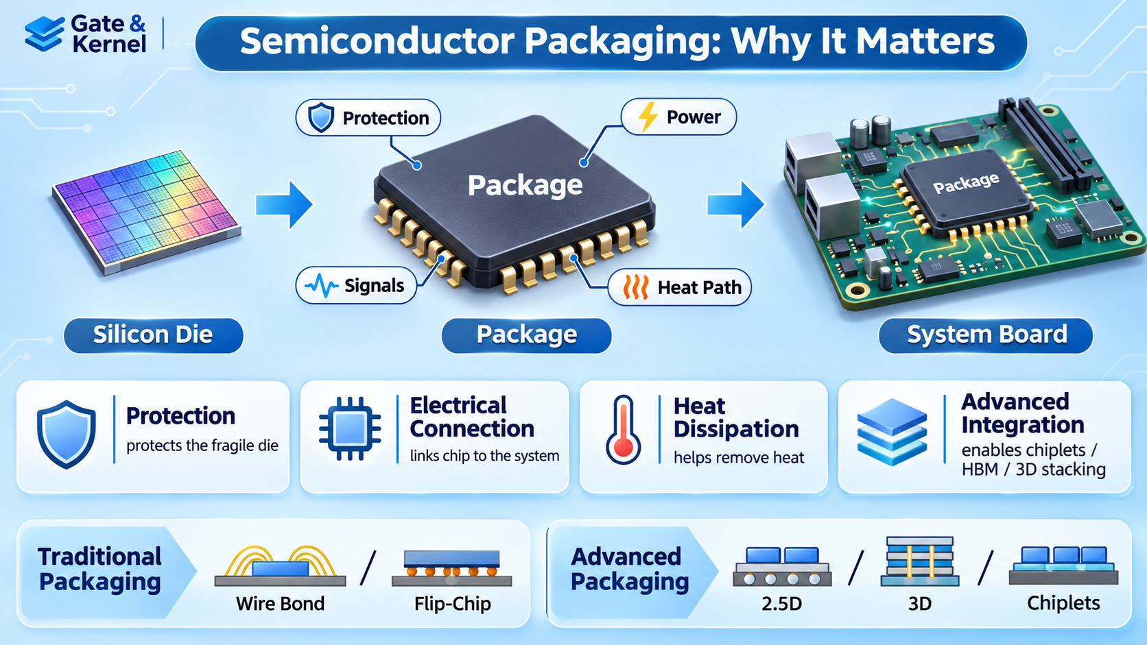
When we think about semiconductor technology, we usually focus on transistors, silicon wafers, manufacturing processes, and processor architectures.
However, manufacturing a silicon chip is only part of the process of creating a usable electronic device.
A completed silicon die must be protected, connected to other components, powered, and cooled. This is where semiconductor packaging becomes essential.
Modern chip packaging is no longer simply a protective enclosure.
It has become a critical technology that influences processor performance, power consumption, memory bandwidth, manufacturing cost, and the ability to combine multiple chips into one system.
Understanding semiconductor packaging helps explain why advanced CPUs, GPUs, and AI accelerators increasingly depend on sophisticated packaging technologies.
What Is Semiconductor Packaging?
Semiconductor packaging is the process of enclosing and electrically connecting one or more semiconductor dies to create a usable electronic component.
A silicon die contains the transistors and circuits responsible for processing information.
However, the die itself is small, fragile, and difficult to connect directly to a computer motherboard or other electronic equipment.
A semiconductor package provides mechanical protection, electrical connections, and a path for removing heat.
Depending on the design, a package may contain a single silicon die or several interconnected dies.
For example, a modern CPU package may include processor cores, cache dies, and an input/output die connected through a package substrate.
The package provides the interface between these internal components and the external system.
What Is the Difference Between a Die, Chip, and Package?
The terms die, chip, and package are often used interchangeably in everyday discussions, but they have different technical meanings.
Silicon Die: A small piece of semiconductor material containing manufactured electronic circuits and transistors.
Chip: A general term commonly used for an integrated circuit. Depending on context, it may refer to the silicon die or the packaged semiconductor device.
Package: The physical structure that protects the die and provides electrical and thermal connections to the outside world.
For example, when you see a desktop CPU, the large metal surface on top is usually an Integrated Heat Spreader (IHS), not the silicon die itself.
The actual silicon die is located underneath, connected to a package substrate.
This distinction becomes especially important when discussing advanced chiplet processors that contain multiple silicon dies inside a single package.
Why Do Semiconductor Chips Need Packaging?
A bare silicon die cannot normally be installed directly into a conventional computer system.
It requires several important functions that semiconductor packaging provides.
Mechanical Protection: Packaging protects the fragile silicon die and its electrical connections from physical damage and environmental exposure.
Electrical Connections: The package provides paths for power, ground, data, address, and control signals.
Heat Dissipation: Packaging helps transfer heat from the semiconductor die to a heat sink or other cooling system.
Power Delivery: Modern processors require carefully controlled electrical power. The package distributes power and ground connections to the silicon circuits.
System Integration: Packaging allows semiconductor devices to connect to circuit boards, memory modules, and other electronic components.
As processors become more complex, these functions become increasingly difficult to implement efficiently.
How Is a Semiconductor Chip Packaged?
Semiconductor packaging generally begins after integrated circuits have been manufactured on a silicon wafer.
The wafer contains many individual dies, which are tested and separated through a process called dicing.
The individual dies are then assembled into packages.
A simplified packaging process includes the following stages.
Step 1: Wafer Testing
Manufacturers test the circuits on the wafer to identify defective or potentially usable dies.
Step 2: Wafer Dicing
The wafer is cut into individual silicon dies using specialized equipment.
Step 3: Die Attachment
A die is attached to a package substrate, lead frame, or another supporting structure.
Step 4: Electrical Interconnection
Electrical connections are created using technologies such as wire bonding, flip-chip bumps, or advanced direct bonding methods.
Step 5: Encapsulation and Protection
The assembled device may be protected using molding compounds, lids, or other packaging materials.
Step 6: Final Testing
The packaged semiconductor is tested to verify its electrical operation, performance, and reliability.
The exact manufacturing sequence depends on the packaging technology.
Some advanced packages involve wafer-level processing, multiple dies, or assembly steps performed before individual dies are separated.
What Is Wire Bonding?
Wire bonding is one of the oldest and most widely used semiconductor interconnection technologies.
It uses extremely thin metal wires to connect contact pads on a silicon die to conductive connections in the package.
These wires may be made from materials such as gold, copper, or aluminum.
Wire bonding is commonly used in microcontrollers, sensors, analog chips, power-management devices, and many other integrated circuits.
Its advantages include relatively low cost, mature manufacturing processes, and broad compatibility with different semiconductor products.
However, wire bonding may be less suitable for devices requiring extremely dense electrical connections or very high interconnection bandwidth.
For these applications, manufacturers often use flip-chip or more advanced packaging techniques.
What Is Flip-Chip Packaging?
Flip-chip packaging connects a silicon die to a substrate through an array of small electrical contacts.
Instead of placing the die face-up and connecting it with wires around its edges, the die is turned over so that its electrical contacts face the substrate.
Small solder bumps or other conductive connections establish the electrical interface.
Flip-chip technology allows connections to be distributed across much of the die’s surface rather than only around its edges.
This supports higher connection density and can improve electrical and power-delivery characteristics.
Flip-chip packaging is widely used in high-performance CPUs, GPUs, and other complex integrated circuits.
It also plays an important role in many advanced multi-die packaging technologies.
What Are BGA, PGA, and LGA Packages?
Semiconductor packages use different methods to connect to circuit boards or sockets.
BGA (Ball Grid Array): Uses an array of solder balls underneath the package. BGA devices are normally soldered directly to a printed circuit board and are widely used in laptops, embedded systems, and memory devices.
PGA (Pin Grid Array): Uses an array of pins extending from the package. PGA has been used in various socketed desktop processors.
LGA (Land Grid Array): Uses flat electrical contact pads on the package. In many desktop CPU systems, spring contacts in the motherboard socket connect to these pads.
These terms describe external connection arrangements rather than the internal semiconductor circuits.
A package can use advanced internal technologies while still presenting a conventional BGA or LGA interface to the system.
What Is Advanced Semiconductor Packaging?
Advanced semiconductor packaging refers to technologies that provide higher interconnection density, improved electrical performance, or more sophisticated integration than conventional packaging methods.
Traditional packaging often focused on protecting and connecting a single silicon die.
Advanced packaging increasingly combines multiple dies and additional components inside one package.
This allows engineers to build larger and more capable systems without manufacturing every function on one monolithic die.
Important advanced packaging technologies include 2.5D integration, 3D stacking, chiplet integration, and hybrid bonding.
These technologies are especially valuable for processors that require large amounts of computing power and high memory bandwidth.
What Is 2.5D Packaging?
2.5D packaging places multiple semiconductor dies side by side and connects them through a high-density interconnection structure.
One common approach uses a silicon interposer.
An interposer contains fine electrical connections that allow neighboring dies to exchange information through short, high-density pathways.
For example, an AI accelerator may place a large processing die next to several stacks of High Bandwidth Memory (HBM).
The interposer provides the electrical connections between the processor and memory stacks.
This arrangement can deliver very high memory bandwidth while reducing the need for long circuit-board connections.
TSMC’s Chip-on-Wafer-on-Substrate (CoWoS) technology is one important example of advanced packaging used for high-performance computing.
What Is 3D Semiconductor Packaging?
3D packaging places semiconductor dies vertically rather than arranging all of them side by side.
Vertical stacking allows components to communicate through short connections between layers.
These connections may use through-silicon vias (TSVs), microbumps, or hybrid bonding technologies, depending on the design.
One example is AMD’s 3D V-Cache technology, which places additional cache memory in a vertically integrated arrangement with a processor die.
Another important application is HBM, which stacks multiple DRAM dies to provide high memory capacity and bandwidth within a compact physical area.
3D packaging can improve interconnection density and reduce some communication distances.
However, stacking introduces challenges involving heat dissipation, manufacturing yield, testing, and power delivery.
What Is Hybrid Bonding?
Hybrid bonding is an advanced interconnection technology that directly bonds semiconductor surfaces and electrical contacts together.
Unlike conventional solder-based interconnections, hybrid bonding can create extremely fine-pitch connections between dies or wafers.
It combines dielectric bonding with direct metal-to-metal connections.
This technology supports very high interconnection density and can reduce the physical distance between circuits.
Hybrid bonding is increasingly important for applications such as stacked memory, advanced image sensors, and high-performance processors.
However, it requires precise surface preparation, alignment, and manufacturing control.
Why Is Packaging Important for Chiplets?
Chiplets are smaller semiconductor dies designed to work together inside one package.
For example, a processor may contain separate chiplets for CPU cores, input/output interfaces, and additional cache.
These chiplets must exchange information quickly and reliably.
Advanced packaging provides the electrical connections that allow them to operate together as one computing system.
This approach can improve manufacturing flexibility because different chiplets may be produced using different semiconductor process technologies.
For example, high-performance CPU cores might use an advanced manufacturing node, while input/output circuits use a more mature process.
Packaging makes it possible to combine these different dies without placing every function on one piece of silicon.
However, the advantages depend on packaging cost, interconnect performance, power consumption, and manufacturing yield.
How Does Packaging Affect Processor Performance?
Semiconductor packaging can directly affect the performance of CPUs, GPUs, and other processors.
One important factor is communication bandwidth.
When multiple dies need to exchange large amounts of data, the interconnections between them must provide sufficient bandwidth.
Short, dense package-level connections can support more efficient communication than interfaces that travel longer distances across a circuit board.
Packaging also influences signal integrity, electrical resistance, power delivery, and communication latency.
For example, connecting an AI processor to nearby HBM stacks through an advanced package can provide much higher memory bandwidth than many conventional external memory arrangements.
However, advanced packaging does not automatically eliminate communication delays.
Die-to-die interfaces still consume power and introduce overhead, so processor architects must carefully balance integration density and communication efficiency.
Why Is Heat Management Important?
Modern processors can generate substantial amounts of heat.
If this heat is not removed efficiently, the processor may reduce its operating frequency to remain within safe temperature limits.
The package provides part of the thermal path between the silicon die and the cooling system.
In many desktop CPUs, heat travels from the die through a thermal interface material to an integrated heat spreader, and then through another interface to a heat sink.
Advanced packaging makes thermal design more complicated.
For example, vertically stacked dies may place heat-generating circuits underneath other silicon layers.
Removing heat from these structures can be more challenging than cooling a single exposed die.
Thermal management is therefore a critical consideration in advanced processor packaging.
Why Is Packaging Becoming More Important for AI Chips?
AI accelerators require enormous computing capacity and fast access to large amounts of data.
Modern AI workloads often involve matrix multiplication and repeated transfers of model parameters and intermediate results.
Even a powerful processor can be limited if its memory system cannot supply data quickly enough.
High Bandwidth Memory and advanced packaging help address this problem.
By placing HBM stacks close to processing dies and connecting them through dense interconnect structures, manufacturers can achieve high aggregate memory bandwidth.
Advanced packaging also enables the integration of multiple processing dies into larger accelerator systems.
This makes packaging a central part of AI hardware development rather than simply a final manufacturing step.
What Are the Challenges of Advanced Packaging?
Although advanced packaging provides major benefits, it also introduces significant engineering and manufacturing challenges.
Cost: Advanced substrates, interposers, bonding equipment, and assembly processes can be expensive.
Manufacturing Yield: Integrating multiple dies creates additional opportunities for defects during assembly.
Thermal Complexity: Closely packed or stacked components can be difficult to cool.
Electrical Design: High-speed interconnections require careful management of signal integrity and power delivery.
Testing and Reliability: Manufacturers must test individual dies, interconnections, and completed packages to ensure reliable operation.
Repair and Replacement: When multiple dies are permanently integrated into one package, replacing a defective component may be impractical.
The industry continues developing new materials, bonding techniques, and manufacturing methods to address these limitations.
Will Advanced Packaging Replace Smaller Transistors?
Advanced packaging and transistor scaling are complementary technologies.
Smaller transistors can increase computing density and improve performance or power efficiency, depending on the manufacturing process and circuit design.
Advanced packaging allows manufacturers to combine multiple dies and technologies into more capable systems.
A future processor may use advanced transistor technology for its compute cores while relying on chiplets, interposers, and 3D stacking for memory and other functions.
This combination provides additional opportunities for improving semiconductor systems without requiring every component to be manufactured on the same process node.
Packaging is therefore becoming an increasingly important dimension of semiconductor innovation alongside transistor design and manufacturing.
Conclusion
Semiconductor packaging is the technology that transforms manufactured silicon dies into usable electronic components.
It protects fragile circuits, provides electrical connections, distributes power, and supports heat removal.
Traditional packaging technologies such as wire bonding, flip-chip, BGA, PGA, and LGA remain important across the semiconductor industry.
Advanced technologies such as 2.5D integration, 3D stacking, hybrid bonding, and chiplet packaging enable more sophisticated processors and memory systems.
These developments are particularly important for modern CPUs, GPUs, and AI accelerators, where communication bandwidth, power efficiency, and thermal management strongly influence performance.
Semiconductor progress is no longer determined only by how many transistors fit on a silicon die. How those dies are connected, powered, packaged, and cooled is becoming just as important to the design of future computing systems.