
For more than half a century, the semiconductor industry has followed an extraordinary trend: computer chips have become increasingly powerful as manufacturers have developed ways to place more transistors onto silicon.
This trend is commonly known as Moore’s Law.
Moore’s Law helped shape the development of modern CPUs, GPUs, memory chips, smartphones, and countless other electronic devices.
It also influenced how semiconductor companies planned new products and manufacturing technologies.
But as transistors approach extremely small dimensions and manufacturing costs continue to rise, an important question emerges: Is Moore’s Law still alive, or has it finally reached its limits?
What Is Moore’s Law?
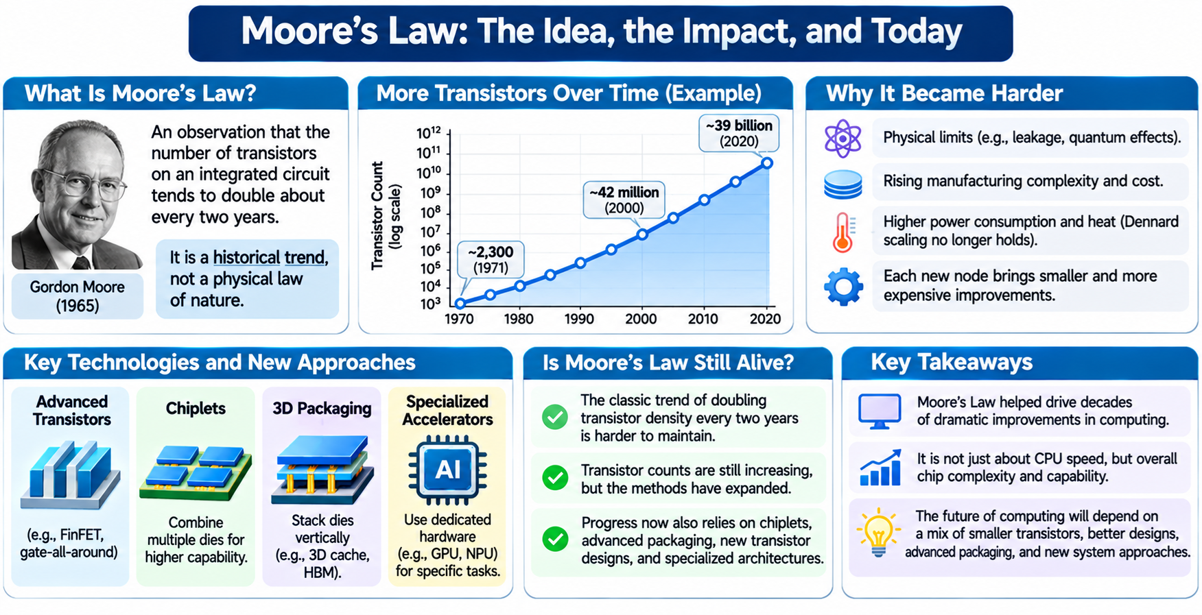
Moore’s Law is an observation that the number of transistors integrated into semiconductor chips tends to increase exponentially over time.
In 1965, Gordon Moore, one of the future co-founders of Intel, observed that the number of components on integrated circuits had been increasing rapidly.
He initially predicted that the number of components per integrated circuit would approximately double every year.
In 1975, Moore revised his projection to approximately doubling every two years.
This later prediction became the commonly cited version of Moore’s Law.
Importantly, Moore’s Law is not a physical law of nature. It is a historical observation and an industry expectation that encouraged continued improvements in semiconductor manufacturing.
For decades, the semiconductor industry invested heavily in research, equipment, and manufacturing processes to maintain this trend.
Why Are Transistors Important?
A transistor is a tiny electronic device that can control the flow of electrical current.
In digital circuits, transistors are used to construct logic gates, registers, memory cells, and other fundamental building blocks of processors.
Modern CPUs and GPUs contain billions of transistors working together to perform calculations, store information, and execute machine instructions.
Adding more transistors allows chip designers to create more complex circuits.
For example, additional transistors can be used to increase CPU core counts, expand cache capacity, add execution units, or integrate specialized hardware such as AI accelerators.
However, doubling transistor count does not automatically double processing performance.
Performance also depends on processor architecture, clock frequency, memory bandwidth, power consumption, and software efficiency.
How Did Moore’s Law Change Computing?
During the early decades of semiconductor development, improvements in manufacturing technology allowed more transistors to fit onto a single chip.
At the same time, smaller transistors often provided improvements in switching speed, power efficiency, and manufacturing cost per transistor.
These advances helped make computers faster, smaller, and more affordable.
Early microprocessors contained only thousands of transistors. Modern high-performance processors can contain tens of billions of transistors, while some advanced multi-die systems contain even more.
The benefits extended beyond desktop computers.
Moore’s Law contributed to the development of smartphones, digital cameras, networking equipment, embedded controllers, and cloud computing infrastructure.
It also helped establish the expectation that each new generation of semiconductor technology would deliver substantial improvements in computing capability.
What Is a Semiconductor Process Node?
Semiconductor manufacturing technologies are commonly described using process-node names such as 28 nm, 14 nm, 7 nm, 5 nm, 3 nm, and 2 nm.
Historically, process-node numbers were more closely associated with physical transistor dimensions.
However, modern node names are primarily technology-generation labels rather than direct measurements of a particular transistor feature.
For example, a 3 nm process does not mean every transistor component measures exactly three nanometers.
Different manufacturers also use different naming conventions, so process-node names cannot always be compared directly.
The more meaningful characteristics include transistor density, performance, power consumption, manufacturing yield, and cost.
Advanced process nodes use increasingly sophisticated transistor structures and manufacturing techniques to improve these characteristics.
Why Is Moore’s Law Becoming Harder to Maintain?
For many years, semiconductor manufacturers improved transistor density by reducing the dimensions of transistor structures.
However, continued scaling has become increasingly difficult.
One major problem is that extremely small transistors are affected by physical phenomena that were less significant at larger dimensions.
These include leakage current, quantum tunneling, electrical interference, and limitations associated with controlling very small transistor channels.
Manufacturing complexity has also increased dramatically.
Advanced semiconductor processes require sophisticated lithography systems, complex materials, and precise manufacturing controls.
As a result, each new manufacturing generation can require enormous investments in research, equipment, and production facilities.
The industry can still increase transistor density, but achieving improvements has become much more expensive and technically demanding.
What Happened to Dennard Scaling?
Moore’s Law is often confused with another semiconductor concept called Dennard scaling.
Dennard scaling describes how shrinking transistor dimensions could allow circuits to operate at higher densities while maintaining approximately constant power density under ideal scaling conditions.
For many years, transistor scaling helped improve both performance and power efficiency.
However, traditional Dennard scaling began breaking down in the 2000s as voltage scaling became increasingly difficult.
This created a major challenge for processor manufacturers.
Increasing clock frequency could produce excessive power consumption and heat.
Instead of continuously raising CPU clock speeds, manufacturers increasingly focused on multicore processors, improved microarchitectures, larger caches, and specialized execution units.
This distinction is important: transistor counts can continue increasing even when clock frequencies and single-core performance no longer improve at their historical rates.
Are Transistors Still Getting Smaller?
Yes. Semiconductor manufacturers continue developing more advanced transistor technologies.
Earlier processors commonly used planar transistors, where the transistor channel was formed along the silicon surface.
The industry later adopted FinFET technology, which uses a three-dimensional fin-shaped structure to improve control of the transistor channel.
More recent manufacturing technologies are introducing gate-all-around transistor designs, including nanosheet structures.
These allow the gate to surround the channel more completely, improving electrostatic control.
Advanced lithography, including Extreme Ultraviolet (EUV) technology, also helps manufacturers create increasingly complex semiconductor patterns.
However, developing smaller transistor structures does not guarantee that every improvement will deliver the same economic or performance benefits as earlier generations.
What Is the Relationship Between Moore’s Law and Chiplets?
Chiplet technology provides another way to increase computing capability without placing every circuit on one monolithic silicon die.
A chiplet is a smaller semiconductor die designed to work with other dies inside a single package.
For example, a processor may combine several CPU compute chiplets with a separate input/output die.
This allows manufacturers to build processors with large numbers of cores while using smaller individual dies.
Chiplets can also be manufactured using different process technologies.
High-performance compute circuits may use an advanced manufacturing node, while input/output functions use a more mature process.
This approach can improve manufacturing flexibility and yield.
However, chiplets do not necessarily increase transistor density within an individual silicon die.
Instead, they allow manufacturers to integrate more total transistors and functionality within a complete processor package.
Can 3D Packaging Extend Moore’s Law?
Traditional transistor scaling primarily increases the number of transistors that fit within a two-dimensional silicon area.
Advanced packaging introduces another approach: stacking semiconductor dies vertically.
Technologies such as 3D integration, hybrid bonding, and through-silicon vias allow multiple layers of circuitry to communicate through dense connections.
For example, additional cache memory can be stacked on a processor die to increase available cache capacity.
High Bandwidth Memory (HBM) uses vertically stacked DRAM dies to provide substantial memory capacity and bandwidth within a compact package.
These technologies can increase system-level integration without requiring all additional transistors to fit on one planar die.
However, 3D packaging introduces challenges involving heat removal, power delivery, testing, and manufacturing cost.
It extends the possibilities of semiconductor integration, but it is not identical to the original transistor-density trend described by Moore’s Law.
Does Moore’s Law Mean CPUs Double in Speed Every Two Years?
No. This is one of the most common misunderstandings about Moore’s Law.
Moore’s Law concerns the growth of integrated circuit complexity, commonly expressed through transistor counts.
It does not state that CPU clock speed doubles every two years.
It also does not guarantee that application performance, energy efficiency, or memory bandwidth will double at the same rate.
For example, manufacturers may use additional transistors to add more CPU cores or larger caches rather than increase clock frequency.
These changes can improve performance for certain applications without producing a proportional improvement in every workload.
Modern CPU performance depends on many factors, including instructions per cycle, core count, cache efficiency, memory performance, and processor power limits.
Therefore, transistor count alone is not a reliable measure of overall computing performance.
Is Moore’s Law Still Alive?
The answer depends on how Moore’s Law is defined.
If Moore’s Law means that semiconductor manufacturers will always double transistor density every two years while reducing cost per transistor, maintaining that historical pattern has become increasingly difficult.
Advanced manufacturing technologies remain capable of improving transistor density, but the economic benefits are less predictable than they were in earlier decades.
If Moore’s Law is interpreted more broadly as the continued growth of transistor counts and computing capability, the semiconductor industry is still making substantial progress.
Modern processors combine advanced transistors, chiplet architectures, 3D packaging, and specialized computing hardware to achieve capabilities that would have been impossible in earlier generations.
The industry is increasingly using multiple technologies rather than relying on transistor shrinking alone.
In this sense, Moore’s Law has not simply stopped. The methods used to sustain semiconductor progress are changing.
What Comes After Traditional Moore’s Law?
Future computing improvements will likely come from several different directions.
Advanced Transistors: New structures and materials may continue improving transistor density and efficiency.
Chiplet Architectures: Modular processor designs can combine multiple dies and different manufacturing technologies.
3D Integration: Vertical stacking can increase component density and shorten certain communication paths.
Specialized Accelerators: GPUs, NPUs, and other dedicated circuits can perform specific workloads more efficiently than general-purpose CPUs.
Improved Memory Systems: Larger caches, HBM, and new memory architectures can reduce data-access bottlenecks.
Software and Architecture Improvements: Better algorithms, compilers, and processor designs can improve performance without requiring proportional increases in transistor counts.
These developments suggest that future semiconductor progress will depend on improvements across entire computing systems rather than only on smaller transistor dimensions.
Conclusion
Moore’s Law began as Gordon Moore’s observation that integrated circuit complexity was increasing exponentially.
For decades, this trend helped drive the semiconductor industry toward smaller transistors, more powerful processors, and increasingly affordable computing technology.
However, transistor scaling has become more difficult because of physical limitations, rising manufacturing complexity, and increasing costs.
Modern semiconductor companies continue improving transistor density, but they also rely on chiplets, advanced packaging, 3D integration, and specialized architectures to increase computing capability.
Moore’s Law is not simply dead or alive in its original form.
Its historical economic and scaling assumptions face growing challenges, while semiconductor innovation continues through a wider range of technologies.
The future of computing will depend not only on how many transistors engineers can place on a chip, but also on how intelligently those transistors are designed, connected, powered, and used.