
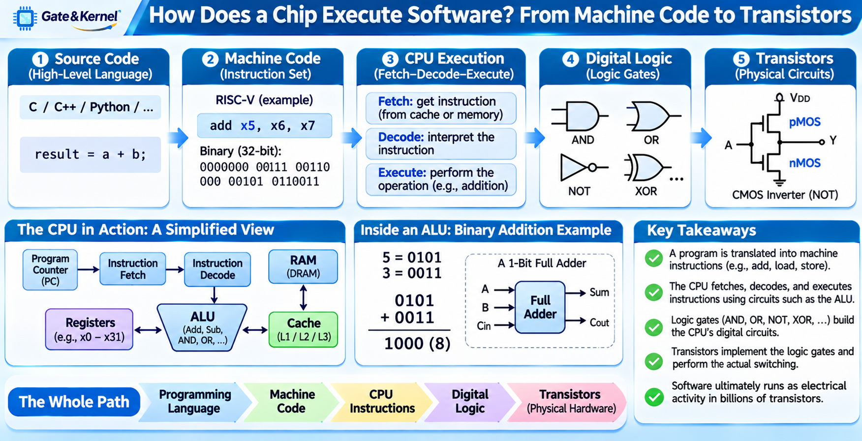
When you open a web browser, play a video, or run a computer program, billions of transistors inside your processor work together to execute software instructions.
But how does a program written in a language such as C, C++, or Python become electrical activity inside a silicon chip?
The answer involves several layers of computer technology, including programming languages, machine code, instruction sets, CPU registers, logic gates, and transistors.
Understanding these layers reveals one of the most important principles of modern computing: software is ultimately executed by physical electronic circuits.
1. Software Begins with Instructions
Software is a collection of instructions that tell a computer what operations to perform.
Programmers usually write software using high-level programming languages such as C, C++, Rust, Java, or Python.
For example, consider a simple C statement:
result = a + b;
This instruction asks the computer to add two values and store the result in a variable.
However, a CPU does not directly understand C source code.
The program must eventually be represented as machine instructions compatible with the processor’s Instruction Set Architecture (ISA).
For compiled languages such as C, a compiler translates source code into machine code. Other languages, including Python and Java, may use interpreters, virtual machines, or just-in-time compilation.
Regardless of the programming language, the processor ultimately executes machine instructions.
2. What Is Machine Code?
Machine code is the binary representation of instructions that a processor can execute.
Each machine instruction follows rules defined by the CPU’s Instruction Set Architecture.
Common processor architectures include x86-64, ARM, and RISC-V.
These architectures use different instruction encodings, registers, and programming conventions.
For example, a RISC-V processor can execute the assembly instruction:
add x5, x6, x7
This instruction tells the CPU to add the values stored in registers x6 and x7 and write the result into register x5.
In the RV32I and RV64I base integer instruction sets, this particular instruction has the 32-bit machine-code encoding:
0000000 00111 00110 000 00101 0110011
The binary fields identify the operation, source registers, and destination register.
The CPU’s instruction decoding hardware interprets these bits according to the RISC-V ISA.
The important distinction is that assembly language provides a human-readable representation, while machine code provides the encoded instructions used by the processor.
3. How Does the CPU Fetch Instructions?
Before executing an instruction, the processor must obtain it from memory.
When a program runs, the operating system establishes the program’s execution environment and makes its instructions and data available through the memory system.
The CPU uses a special architectural register called the Program Counter (PC), or Instruction Pointer in some architectures, to identify the next instruction address.
A simplified instruction-fetch process works as follows:
- The CPU identifies the next instruction address.
- The memory system supplies the instruction, often from the instruction cache.
- The processor decodes the instruction.
- Execution hardware performs the requested operation.
- The processor continues with another instruction.
This is commonly described as the fetch-decode-execute cycle.
Modern processors overlap many of these operations using pipelines, prediction, and other techniques. Therefore, instructions do not necessarily pass through every stage one at a time.
4. How Does the CPU Decode Machine Code?
A machine instruction contains binary fields that describe what the processor should do.
These fields may specify an operation, registers, immediate values, or memory addressing information.
For example, an addition instruction may identify two source registers and one destination register.
The processor’s instruction decoder interprets the machine-code bits and produces internal control information.
This information directs the appropriate execution resources to perform the operation.
Some modern processors, particularly high-performance x86 CPUs, translate architectural instructions into simpler internal micro-operations before execution.
Other processors may decode instructions more directly into execution controls.
The internal implementation differs between processor designs, but the architectural behavior must follow the ISA specification.
5. How Does the ALU Perform Calculations?
One important execution component inside a CPU is the Arithmetic Logic Unit (ALU).
The ALU performs integer arithmetic and logical operations.
Common operations include addition, subtraction, AND, OR, XOR, and comparisons.
Consider adding decimal numbers 5 and 3.
In four-bit binary:
5 = 0101
3 = 0011
The addition is:
0101 + 0011 = 1000
The result, 1000, represents decimal number 8.
Inside the ALU, digital circuits calculate the result using binary logic.
One basic building block is the full adder, which accepts two input bits and a carry-in bit, then produces a sum bit and a carry-out bit.
Multiple adder circuits can be combined to perform arithmetic on larger binary values.
Modern CPUs use more sophisticated adder structures to achieve high performance.
6. How Do Logic Gates Perform Operations?
An ALU is built from digital circuits containing logic gates.
Logic gates implement basic Boolean operations, such as AND, OR, NOT, and XOR.
For example, an AND gate produces a logical one only when both inputs are one.
An OR gate produces one when at least one input is one.
An XOR gate produces one when its two inputs differ.
These simple operations can be combined to create more complex circuits.
For example, a full adder uses logical operations to calculate binary sums and carries.
Logic gates are also used in instruction decoders, registers, memory interfaces, counters, and control circuits.
Although modern processors contain extremely complicated hardware, their digital behavior is constructed from combinations of these fundamental operations.
7. How Do Transistors Implement Logic Gates?
Logic gates are physical electronic circuits built using transistors.
A transistor is a semiconductor device that controls electrical current.
Modern digital processors primarily use CMOS technology, which combines n-channel and p-channel MOS transistors.
These transistors act as electronically controlled switches.
For example, a CMOS inverter, which implements the NOT operation, can be constructed using one p-channel transistor and one n-channel transistor.
When the input is logically low, the output is driven high. When the input is logically high, the output is driven low.
The circuit therefore reverses the logical state of its input.
More complex transistor arrangements implement NAND, NOR, and other logic functions.
By combining many such gates, engineers construct arithmetic units, registers, decoders, and complete processors.
This establishes the physical connection between binary instructions and semiconductor electronics.
8. What Role Does the CPU Clock Play?
Most modern CPU execution circuits operate using clocked digital logic.
A CPU clock provides repeating timing signals that coordinate state changes within the processor.
For example, a processor operating at 4 GHz has approximately four billion clock cycles per second.
However, this does not mean it executes exactly four billion instructions per second.
Some instructions require multiple clock cycles, while modern processors can complete multiple instructions during one cycle.
Clock signals coordinate registers, pipeline stages, and many other synchronous circuits.
Combinational logic, including portions of an ALU, produces outputs based on its current inputs without requiring a clock transition for every individual gate operation.
The clock helps determine when results are captured and made available to subsequent processing stages.
9. How Do Registers Store Results?
Registers are small, fast storage locations used by the CPU to hold values, addresses, and intermediate results.
When an ALU performs an addition, its result may be written into a destination register.
Registers are implemented using circuits capable of retaining binary states while power is supplied.
In many synchronous designs, flip-flops capture input values at specified clock transitions.
For example, when the RISC-V instruction add x5, x6, x7 executes, the processor reads the values associated with x6 and x7, performs the addition, and updates the architectural value of x5.
Modern processors may use physical register files, register renaming, and instruction retirement mechanisms internally.
These techniques improve performance while preserving the behavior required by the ISA.
10. How Does the CPU Access RAM?
A processor cannot store an entire operating system and all application data in its internal registers.
Instead, programs and data are primarily maintained in system memory, or RAM, while they are being used.
When the CPU requires information from memory, a load instruction initiates a memory access.
The processor typically checks its cache hierarchy before accessing DRAM.
L1 cache provides very fast access to a relatively small amount of information. L2 and L3 caches provide additional storage capacity with different latency characteristics.
If the requested information is not available in the relevant caches, the memory subsystem may send a request to the integrated memory controller.
The memory controller coordinates communication with DRAM and returns the requested data.
Store instructions work in the opposite direction, updating memory through the processor’s cache and memory system.
This hierarchy allows modern CPUs to avoid many slow RAM accesses.
11. How Does Software Control Hardware?
Software does more than perform arithmetic calculations.
Programs also interact with hardware devices such as storage controllers, network adapters, displays, keyboards, and sensors.
Operating systems provide interfaces that allow applications to request these services.
For example, when an application reads a file, it normally asks the operating system to perform the operation.
The operating system communicates with the appropriate device driver, which controls the hardware.
Many hardware devices expose control registers through memory-mapped I/O.
These registers allow software to configure devices, start operations, and read status information.
For example, an embedded processor may write a value to a hardware control register to activate an output pin.
The processor executes machine instructions, and the resulting electrical signals cause the hardware state to change.
This principle is fundamental to microcontrollers, embedded systems, and computer peripherals.
12. How Can Billions of Transistors Work Together?
Modern processors contain billions of transistors, but they do not operate as billions of independent devices controlled directly by software.
Instead, transistors are organized into logic gates, storage elements, and larger functional blocks.
These blocks form registers, ALUs, caches, instruction decoders, execution units, and communication interfaces.
A modern CPU may contain multiple cores, each capable of executing its own instruction stream.
Processors also use pipelining, superscalar execution, branch prediction, and out-of-order execution to improve performance.
These features allow many instructions to be processed simultaneously or overlap in different stages.
The ISA defines the architectural behavior visible to software, while the microarchitecture determines how the hardware implements that behavior.
This distinction allows different processors to execute compatible machine code while using very different internal circuit designs.
13. Does Software Directly Control Every Transistor?
No. Software does not individually switch billions of transistors.
A program specifies operations using machine instructions.
The CPU’s existing circuits interpret those instructions and generate the electrical activity needed to perform them.
For example, an addition instruction selects arithmetic hardware, supplies operand values, and causes the result to be captured according to the processor’s execution design.
The individual transistor transitions occur as a consequence of the circuit structure and electrical signals.
Software controls the processor through the instruction interface, not by directly programming the behavior of each transistor.
This is an important difference between executing software on a CPU and configuring digital hardware in an FPGA.
In a conventional CPU, the hardware execution structure is already manufactured. Instructions determine which operations that hardware performs.
In an FPGA, configuration data can change how programmable logic and routing resources are connected, allowing the device to implement different digital circuits.
Conclusion
A computer chip executes software through a sequence of transformations between programming concepts and physical electronic operations.
High-level programs are compiled, interpreted, or otherwise translated into operations that ultimately involve machine instructions.
The CPU fetches and decodes those instructions, uses execution units such as the ALU to perform calculations, and stores results in registers or memory.
Logic gates implement the required Boolean operations, while transistors provide the physical switching behavior that makes those circuits possible.
Clock signals coordinate much of the processor’s activity, and memory systems supply the instructions and data needed for execution.
The complete relationship can be summarized as: Programming Language → Machine Code → CPU Instructions → Digital Logic → Transistors.
This is how software becomes physical activity inside silicon, allowing billions of tiny electronic devices to work together as a programmable computer.